Orcad Layout communicate interactively with Capture.Este chapter explains how to use Capture to Layout to annotate direct, inverse and crossmatch.
When making changes to the board in Layout, you can reverse an annotation on that information to Capture utiizando Backannotation File option. (SWP) in the Generate Reports dialog box in Layout.
Select the option Run Eco to Layout dialog box in the Create Netlist from capture to automatically communicate changes made to the layout design in Capture. If the ficherode Layout is open when you update the links file, Layout monsters a dialog box asking if you want to upload the new file connections. If the layout file is not open when you change the list of connections, layout will make that question when you open the new file layout.
Can also cross-evidence; Layout.Con capture and crossmatching, can select a part or a connection page in Layout Captureo scheme is a three-part proces
To generate a list of connections in the layout format.
-Create a plate layout. You can also transmitirinformacion concerning the parts, connections and pins, creating user-defined properties in the parts, connections, or pins.
Maintain the integration between the plate layout and design in Capture requires Tares are performed periodically following:
-create a file retroanotación of ORCAD (. SWP)
-Make a notation reverse Capture using retroanotacion file.
Use the command auto-echo of an annotation to Layout directade any edits made to the design in Capture to Layout.
Added or deleted any connections on the board in Layout Capture.Por not be listed on the right when you want to change connections, make changes and make a notation Capture directly in Layout.
designated reference changes must be made in retroanotados in Layout and Capture.
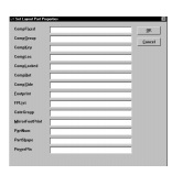
To prepare a design capture for use in Layout, rpimero must modify the design by assigning a special rpopiedades library components that support layout for all parties. Tables in this section lists the properties of each part, supported by pin connection or Layout. These three dialog boxes (Set Pin Layout Properties) appear when selecting their corresponding commands in the menu page editor Framework Schema.
1-Create a design in Capture
2-Assign values to appropriate properties in the dialog box Set Layout Part Properties dialog box Net Set Layout Properties dialog box or the Set Layout Pin Properties.Estos values of the transferred information, the connection or pin a Layout.
3-Map of PCB component library for each of the parties. Use only compatible components layout, by selecting custom component libraries.
4-If you are using parts other than libreías Layout, such as discrete parts and components, verify that the numbers of the pins match the pin numbers of the component library in the PCB. You may have to work with the editor of parts of Capture or libnrerias the Layout editor. You shall ensure that each pin has a pin number as well as a pin name.
5-Run Rule desing Chek (in the nemu Tools) to check the electrical rule violations.
Transferring user-defined properties to Layout
To transfer information of parts, connections, or pins to Layout, assign values to the appropriate prpopiedades dialog boxes Part Set Layout Properties, Set Net Properties Layout and Pin Set Layout Properties.
For the properties dialog boxes are added to the parts, connections, or pins, you need to have selected the appropriate objects on the page of the schema before running any of the three marcros.
The value entered for each property, you must be uppercase.
Add properties Layout parts of a party
1-Select a party to a page of a schema.2-In the Setting menu, Select Part Properties.Se Set Layout dialog box displays Set Layout Part Properties.3-Enter values for those properties that want to add to the party, after click on OK. The properties will be added to the party.
1-Select a link on a page layout.
2-Setting menu, select Set Layout Properties.Se Net dialog box will display the Set Layout Net Properties.
3-Enter the values for those properties to be added to the link, then click on OK.

1-Select a pin on a page in an outline.
2-In the Macro menu, choose 'Set Layout Pin Properties.Se display the dialog box Pin Set Layout Properties.
3-Enter values for those properties that want to add to that pin, then click on OK.Las properties are added to this pin.

After the design deprpara Capture and that this is free of the rules violacones Electric, may create a netlist file (MNL) for use in existing Layout.Debera LAYOUT.INI file a copy in the same directory as CAPTURE. EXE to generate the list of connections.
-To create a list of connections and use it in Layout:
1-open design Capture.
2-On the Tools menu, select Create Netlist. This displays the Create Netlist dialog box.
3-Click on the Layout tab. It will show the Layout tab.
4-In grupoPCBFootprint box, make sure {PCB Footprint} appears in the text box Properti Combined string.
5-In the Netlist File text box, make sure the path to the file from the list of connections is making correcto.La netlist design ell Capture name and adds the extension.MNL
6-Click on OK. Capture processes the list of connections and create a fichero.MNL directorioespecificado that saved in the previous step.
Scoring dela reverse plaque from layout
When adding new parties to capture, use the option Incrementalreference update in the dialog box Parts Reference Update (as opposed to the option Unconditional reference update) when upgrading high benchmark of the parties.
In Layout, you can make a notation reverse the changes of the plate to Capture using the file (. SWP). Once created the file .. SWP, the current file layout stop salvcara intercambio.Se contain information of a copy of the file of the nameplate BACKANNO.MAX
Acer inverse annotation
1-Auto In the Layout menu, select Back Annotate. It will show a dialog box asking if you want to save the layout design. Saving the design will remain the link between layout and capture.
2-In Capture Tools menu, select Back Annotate.
3-Make sure the option is enabled Entire Process desing.
4-select the Browse button. Locate and select the file created in Layout reverse entry (Name _del_diseño.SWP), and click OK. Layout information will be recorded in the design in Capture.
Direct data annotation scheme to Layout
Devera be a copy of the file directory LAYOUT.INI Layout in the same directory where this CAPTURE.EXE for the direct annotation layout correctly.
"To make a direct annotation
1-In Capture Tools menu, select Create Netlist. Will display the dialog box Create Netlist.
2-Select the Layout tab, after click on OK.
3-session In the Layout area, select Tools then ECO, then one of two options of Auto ECO.Se display the File dialog box A.
4-Select a fichero.MAX that informaciondel want to add the new scheme, then selecting the Open button. Will display the dialog box Output report.
5-Find and select the list of connections (MNL) created in step 2, then select the Open button. Will display the dialog box Output report.
6-Specify the name for the output report (usually nombre_del_diseño.LIS) and a location. The output report is shown in a text editor and the dialog box will appear Merged Output Binary.
7-Specify a name and location for the combination plate, then select the Save button. Layout combine the files based on the type of ECO Auto selected.
8-Read the output file cuidadosamente.Los changes listed here must agree with the edits made to the design in Capture.
In the layout, as usual, start menu-> Programs -> orcad -> layout plus.

After opening the new file program and click in a window will appear that way.

Here are two paragraphs FILE NAMES and OPTIONS, OPTIONS leave it as is and focus on the three radio buttons (BROWSE) that we have the right, first select the configuration file layout that will leave the default one (default.tch) in the second we choose the location of the MNL file you just created to capture cis and the third will tell you the name and location of the file will be created, which have the MAX extension.
El sistema para buscar el footprint adecuado es parecido a buscar el componente en el capture, en cuanto le hemos dado a apply eco lo que hace es “linkar” los nombres de los componentes del capture a los fooprint de las librerías que tiene el layout (en este zip tenéis algunas librerías para añadir al layout, solo tenéis que copiar y pegar el la carpeta libraries del layout plus).
When the layout does not find the footprint we leave this little screen,

In this particular tells me that the footprint of the component is called J1 phonejack_stereo and select one of the options to choose from is the first, linkar an existing footprint with the component, the other two options are for people who are placing on the orcad issue, which is not my case.
Now we have a screen like this

Here, the first thing arem be sure they're all the libraries available and it will select the Add after which we asked which library we want to add, select all and welcome.
Fact that what remains is the same as above in the capture, select all the libraries of the listbox (it will in a dark tone as selected) and in the text field will introduce the name of what we want, spend as capture that in the footprint position themselves in alphabetical order of the letters entered.
In the box bigger, if we select a footprint, it will appear the picture of the component, not so with the measures of the same, there is the difficulty of matching the right one, since there are pictures the same but with different measures.
Another difficulty comes when we have no idea how the footprint can be called so as we capture in a search option.

When you select Add, and we give back to the previous window, which we have done is select the library and the component so we'll have the drawing of the screen described above, if the component is not looking for but if the right family we do is move one by one by each component to find the right one, usually each library covers a family of components, so that selecting an approximate description of the similar components will get all of that family and will issue time to find the right one.
We do this for each component, only the once arem is recorded as the ratio of all components.

The process of moving the pieces is very simple, in the toolbar


--- End command ends with the option you have selected.
---------------- Add adds a new connection between pins.
------------- Delete Deletes a line or connection between two pins.
Disconnect pin pin ---- Disconnect all connections arriving or leaving.

This example is microcontroller with LCD, jumpers, switches, buttons and chips to program it and see the results of these porgramas stabilized.
Now what arem will give you a plaque area (yellow line), which for this command is used


First select the width of the tracks that this will have to go to the menu
windows-> Nets


To tell you the faces that can be used for tracks and bridges will not go to menu Tool-> Layer-> select from speadsheet ..


Choose layer "Top" and return to the menu properties, this layer is the front so we will tell you to use to route by checking the option "Routing layer", if the plate is double-sided use also select "Bottom and arem same. Now select one or more layers for use by the bridge, I usually use single-sided plates thus assigned to layer "Top " routing and "Bottom" bridges.
To assign the layer as a bridge, arem exactly the same, but select the "Layer Jumper. "
They are already mapped layers will now have to enable the bridge, go, tell him he can use. This will not go to File-> Load and locate the folder where the layout has the data files, which by default is usually in C-> OrCAD-> OrCAD_10.3-> tools-> layout_plus-> data and we will have the file loads and jumper_v.sf jumper_h.sf, one for horizontal jumpers and one for vertical.
This must be done always, is not recorded, but open the same project previously loaded these files do not save the layout, so you have to back loaded. And now if we can now route the board, so we'll go to the Auto-> autoroute-> board. Time is relative in relation to the complexity of the board and we remain well

If plaque is complex and has been used Orcad bridges, some of these lines have a marked in red, those are the bridges. If you see a line that is too board or not
you like like this and want change, you have to use the tool
Add / Edit Route mode "operation of it is equal to the tool conection tool" we use for connecting components. Once you taste this to your print is only photolith, select the window is already open, "Post process" in order to have two windows open, the plate and the post process which will minimize arem everything and restore only those two so you do not go to the menu window and select Tile.
Now, in the "Post Process" select "top"and with the right mouse button down and select "preview. "


No hay comentarios:
Publicar un comentario