DESCRIPTION
XC9572 CPLD implement in a 1-bit full adder.
ANALYSIS
Its truth table is:

On your desktop find the icon 'Project Navigator', open it.

*- It is divided into four windows:
In the upper left corner shows the various sources of design.
Below, the Process window displays the list of
processes available to the source selected in the top window.
The third window is located at the bottom of the screen. This is the console messages, which
updated information and warning messages.
The last window is positioned on the right and is an editor of HDL.
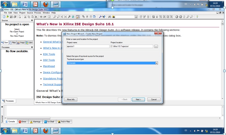
First, locate the directory where we will locate the project 'C: \ Xilinx71i_WEBPACK \ bin \ Projects', write the name of the project' add1 'and at the same time, we created a folder on the previously chosen directory'C: \ Xilinx71i_WEBPACK \ bin \ Projects \ add1 ', and finally, select the input type of project, in our case would be graphic.

+ Device Family: We can choose to use CPLD family. Select XC9500 CPLD's
+ Device: Select the CPLD family specifically chosen. In our example 'XC9572'.
+ Package: Select the encapsulation type. We chose the 'PC84'.
+ Speed Grade: Select the operation speed of the CPLD. The data comes in nano seconds and referred to
pin to pin delay. The selection depends on the device we have, in our case we choose '-7'.
+ Design Flow: In this section, select the type of input (Schematic), the synthesizer (XST for
VHDL) simulator (ModelSim) and used the simulation language (VHDL).

In the window that shows off, select the template 'Schematic' and assign a name to the source, in our case will 'add1bit'. The option to 'Add to project' must be enabled.

It creates the following report:


ADDING COMPONENTS:
We click on the 'Symbols' and opens the window of symbols, showing the libraries and their corresponding components.

Selecting 'All Symbols' and typing 'xor2' at 'Symbol Name Filter'. Then drag the
symbol with the mouse to place it in the desired location within the schematic.
The other way is to select the category 'Logic' and typing 'xor2' at 'Symbol Name Filter' or
looking directly into the library. Subsequently, we drop the symbol with the mouse to
place it in the desired location within the schematic.

From the menu bar, select 'Add-> Wire' or click on the icon on the toolbar.

Write the name 'A' in box 'Name' can see how the mouse cursor
add the name 'A' and clicking the line you want to name, this will take the name.
The 'I / O Markers' can be input, output, or bidirectional, so we must choose the type of mark prior to placement.
To place a check mark placed just above the name of the net and clicking. In the case of not having been named the net, the 'ECS' put a name with reference to internal parameters.

Before proceeding with the process, it is advisable to check the errors that have been committed in connection-level design. We click on the icon in the toolbar.
FILE-CREATE THE BENCH TEST WAVEFORM:
The test bench is a VHDL file in which the entity instance that you want to test 'uut' (unit under test).
This unit will apply a set of test vectors (stimuli) into a text or graphic, which is called the expected output. Subsequently, from the "ModelSim", compares the solution offered by the 'uut' with the expected output, and if not equal is that there has been an error.
Therefore, the first step is to create the test bench file. Right-clicking on the file 'add1bit.sch' select the option 'New Source'. On the next screen choose the option of 'New-> Test Bench Waveform', and call it 'tb_add1bit'.
Our design does not have a clock as an input select to perform simulación'Combinatorial combinational (or internal clock). "
Delay times we leave the default, ie 50ns will check exits after being assigned entries and assign new entries after being checked 50ns output.

Now 'HDL Bencher' is open to us within the surroundings 'ISE' onda.En forms showing our case, we will verify the truth table of full adder for a bit. To do this, will put the
stimuli by clicking the left mouse button over the blue background of the starters to perform any combination of the table in the horizontal timeline.

Outputs, yellow background, we could put the expected value in each of the combinations or, on the contrary, wait for the simulator itself give us the answer. We will not value.
Then save the waveforms and close the 'HDL Bencher. "
We can see we have been associated test file 'tb_add1bit' to file 'add1bit.sch', in addition, the test bench file carries a set of process related.
FUNCTIONAL SIMULATION ModelSim;
In the next figure we can see is the "Project Navigator" and part of the file content
'tb_add1bit_tb.vhd'.

Having selected the font 'tb_add1bit-testbench_arch [tb_add1bit_tb.vhd]', press twice on the process' Simulate Behavioral VHDL Model. "This will launch the associated application simulation 'Project Navigator', in our case 'ModelSim XE III v6.0a. "The simulation will run automatically giving
result in the console 'ModelSim':

line. In the 'Help'from 'ModelSim' we can find a PDF file with a description of all
we can use commands in the console.

CONTROL SIMULATION

SIMULATION ANALYSIS
It only remains to make the simulation analysis.


to be used. Also suggests the possibility of setting it automatically, so
respond, 'If
Pin assignment with PACE (Pin-out Area Constraints Editor), process associated with the file
restrictions 'add1bit.ucf'.


Make all necessary steps to convert the input netlist file in a proprietary format NGD using an internal representation of the technology being used. This file describes the design in terms of logic (logic gates, decoders, RAM's, flip-flop's, etc).
To run the utility we get up 'Translate' and double click.
CONEXIONADDO ((FFiitt))
Fit maps the logic defined by the NGD file into the CPLD resources, such as logic cells, I / OB 's and other components. The process output is a file that is physically VM6 connection of the components in the CPLD. To run the utility we get up 'Fit' and double click.


HW-USB cable is designed to run under Windows as long as they have been installed on the design environment 'ISE'.
Must be connected to a USB 2.0 port for Hi-speed operation. (In a USB 1.0 port has limited its maximum operating speed)

And he shows 'IMPACT'. By default, is configured with a clock speed for the download of 6 Mhz.

Erase Delete Befote .- CPLD Programming before programming.
Verify Verify .- CPLD programming.
Read Protect .- Protects against Reading after programming CPLD
Write Protect .-Write protect after programming the CPLD.
Functional Test .- Perform a test of programming. To do this, you need a file with test vectors.


Input / Output
